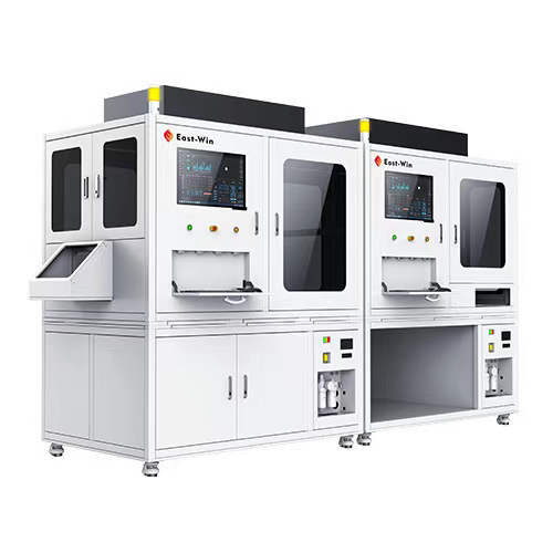
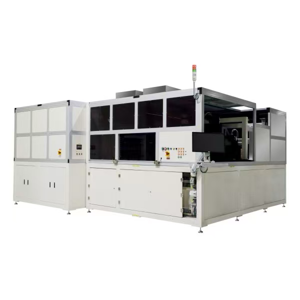
In the three major high-tech manufacturing fields of robotics, semiconductors, and precision electronics inspection, existing mainstream solutions (such as visible light inspection and traditional electrical probe testing) have reached their physical limits. The introduction of high-order Ir thermal imaging (VGA, SXGA, or higher) is not just an optimization, but a fundamental breakthrough in achieving functional, non-contact, and real-time inspection.
I. Five Core Advantages of Ir Thermal Imaging Compared to Existing Solutions
High-order Ir thermal imaging, with its unique capabilities, provides functional data and non-contact advantages that are unmatched by existing technologies:
- Achieving functional testing: Ir thermal imaging can monitor the heat dissipation of components in real time when they are powered on or in operation. In contrast, existing solutions are mostly structural or electrical tests, which can only detect design defects or open/short circuits, but cannot detect subtle current leakage, impedance unevenness, or early thermal stress defects.
- Absolutely non-contact: It achieves temperature measurement at the micrometer level without probe contact. Traditional probe testing can cause mechanical stress damage or affect the true electrical characteristics of components. Thermal imaging completely avoids physical interference, making it particularly suitable for delicate components such as FPCBs and MicroLEDs.
- Comprehensive scene visualization: Capable of capturing the complete thermal scene distribution of an entire circuit board, wafer, or robot joint in one go. Traditional probes or thermocouples can only measure the temperature at a single point and cannot provide a global view of thermal uniformity and thermal bridging.
- Transmittance and Transparent Media Analysis: This technique allows observation of internal component heat generation by penetrating part of the encapsulation material or a transparent medium (such as a glass panel). Visible light cannot penetrate opaque encapsulations. Thermal imaging can indirectly monitor the functional status of hidden components.
- Ultimate predictive maintenance: By capturing temperature differences at the millidegree level under extremely low NETD (thermal equivalent temperature difference), early fault warnings are achieved. Traditional solutions can only detect problems after a failure occurs or performance degrades significantly, while thermal imaging can make predictions hours to days in advance.
II. Key Needs in Three Major Areas: Applications Where Ir Thermal Imaging is Essential
The following key points are inspection and maintenance tasks that cannot be effectively addressed by existing technologies and must rely on thermal functional data provided by high-order Ir thermal imaging:
- 🔬 Essential needs in the semiconductor and PCB/FPCB testing fields
- ⚡ Micrometer-level current leakage fault location:
- Key concern: Current leakage (i.e., micro-short circuits or impedance anomalies) caused by tiny defects with nanometer-wide linewidths on the chip or PCB. This leakage generates very little heat, but it is a major factor affecting chip stability.
- Why is it necessary? Traditional electrical testing can only measure overall power consumption and cannot pinpoint specific micron-level heat-generating units. Ir SXGA level testing, combined with a high-magnification optical system, is the only technology capable of precisely locating these millimeter-level hotspots without contact.
- 🔄 FPCB Stress Testing and Fatigue Inspection:
- Essential requirement: Reliability of internal circuit connections on flexible circuit boards under bending and operational conditions.
- Why is it necessary? Only thermal imaging can display the uniformity of line impedance in bending areas in real time while the FPCB is running. Any internal delamination, microcracks, or solder fatigue will immediately manifest as localized hot spots, which other non-contact methods cannot observe.
- 📺 Essential needs in the field of MicroLED and high-end panel testing
- 🌡️ Screening for Functionality and Thermal Uniformity of MicroLEDs After Mass Transfer:
- Essential requirement: After transferring millions of MicroLED chips to a substrate, it is necessary to test the functionality, current distribution uniformity, and thermal decay consistency of each individual chip.
- Why it's essential: Ir SXGA or higher resolution is the only tool that can simultaneously measure and compare the real operating temperatures of millions of micrometer-level pixels without contact. It can quickly screen chips with thermal defects, uneven heating, or potential lifespan issues.
- ☀️ Correlation analysis of the optical and thermal properties of the panel:
- Essential requirement: Evaluate the correlation between brightness and heat distribution in OLED or Mini/MicroLED panels. Heat is a key factor affecting display lifespan and color uniformity.
- Why it's necessary: Thermal imaging provides functional images and is the only tool to verify the thermal design of the drive circuit and monitor the relationship between light efficiency and thermal stability in real time.
- 🤖 Essential needs in the fields of robotics and industrial automation

- ⚙️ Real-time predictive maintenance of critical robot components:
- Essential requirement: Early warning of wear and tear on motors, reducers, or bearings inside the joints of robotic arms and collaborative robots on high-speed automated production lines.
- Why it's essential: Frictional heat caused by mechanical wear is the first sign of any failure. Ir thermal imaging can continuously monitor the temperature profiles and localized hot spots of critical components remotely and non-contactly. If any abnormal deviations occur, edge AI can immediately issue a shutdown warning, preventing catastrophic failures and high downtime costs. This is a decisive technology for shifting from reactive maintenance to predictive maintenance.
Conclusion: Technological barriers and market competitiveness
The application of advanced thermal imaging (IR) technology in these fields is no longer just an advantage, but a strategic technological barrier for enterprises to achieve high-yield, high-reliability, and high-efficiency manufacturing. Combining powerful edge AI algorithms for real-time defect classification and predictive analysis is an inevitable choice for enterprises to maintain global competitiveness in the Industry 4.0 era.


